Wiring: Complete Connection List
One place to look while wiring. For the per-chip pin diagrams, see Pinout Reference.
Circuit diagrams
Component placement on the breadboard, left to right: the 3.3 V supply, the AS6C62256-55PCN RAM, the W65C02S CPU, and the Raspberry Pi Pico 2. Knowing this order makes the two wiring diagrams below easier to follow.
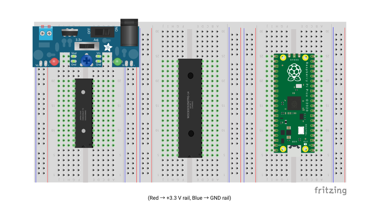
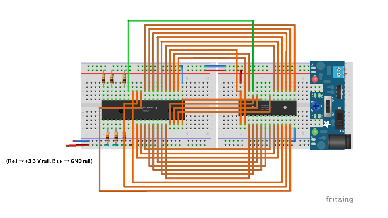
The full wiring is split into two diagrams because routing every net in a single view was unreadable. Both halves share the same 65C02 in the middle; together they form the complete circuit. In both, red = +3.3 V rail and blue = GND rail.
Diagram 1: 65C02 ↔ Pico
The Pico drives the address bus and the ROM data bus, plus RESET and PHI2 (the green wires). Purple wires are the shared A0–A15 / D0–D7 bus; the resistors are the 10 kΩ pull-ups on the 65C02 control inputs.
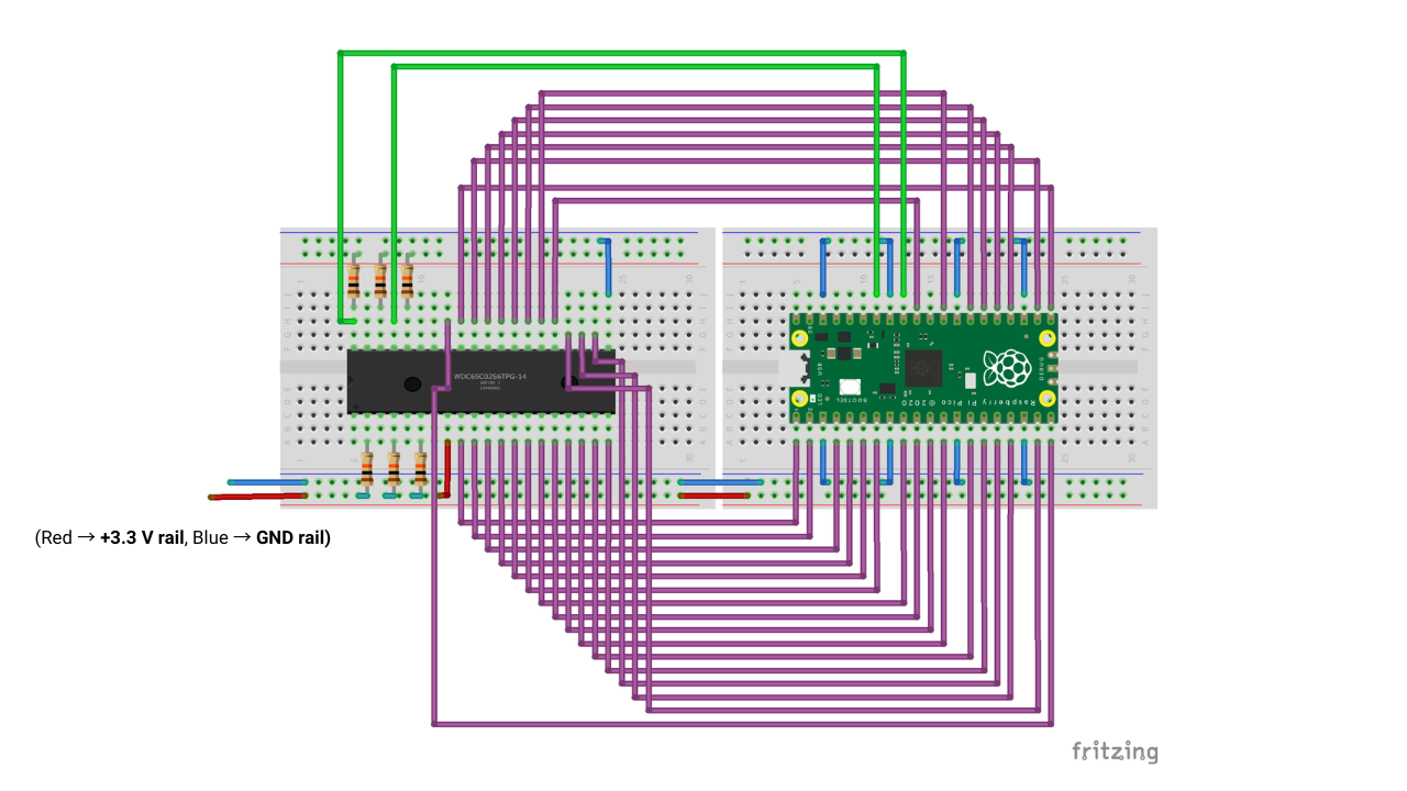
Diagram 2: 65C02 ↔ RAM
The same address and data bus continues from the 65C02 to the AS6C62256-55PCN RAM (orange wires),
with RWB → WE# for writes and A15 → CE# for chip-select. The 3.3 V supply module sits on
the right.
The connection tables below list every net precisely.
Point-to-point connections
From |
To |
Purpose |
|---|---|---|
65C02 pin 34 (RWB) |
RAM pin 27 (WE#) |
Write enable to RAM |
Pico pin 32 (GP27) |
65C02 pin 40 (RESB) |
Reset control |
Pico pin 34 (GP28) |
65C02 pin 37 (PHI2) |
Clock at 1 kHz (default) |
(optional) Pico GP23 |
65C02 pin 34 (RWB) |
Not used for |
RAM pin 22 (OE#) |
+3.3 V |
Outputs disabled, writes only, avoids contention |
Pull-up resistors (6 × 10 kΩ, all top to +3.3 V)
Resistor |
Pulls up |
Why |
|---|---|---|
R1 |
65C02 pin 2 (RDY) |
CPU stalls if RDY floats low |
R2 |
65C02 pin 4 (IRQB) |
Inactive (high) when unused |
R3 |
65C02 pin 6 (NMIB) |
Inactive (high) when unused |
R4 |
65C02 pin 36 (BE) |
Bus always enabled |
R5 |
65C02 pin 40 (RESB) |
High when Pico isn’t asserting reset |
R6 |
65C02 pin 38 (SOB) |
Inactive (high) when unused, cheap insurance |
Leave open
65C02 pins |
Pico pins |
|---|---|
1 (VPB), 3 (PHI1O), 5 (MLB), 7 (SYNC), 35 (NC), 39 (PHI2O) |
30 (RUN), 35 (ADC_VREF), 36 (3V3 OUT), 37 (3V3_EN), 40 (VBUS) |